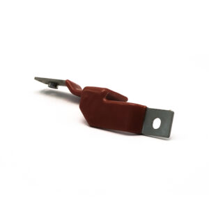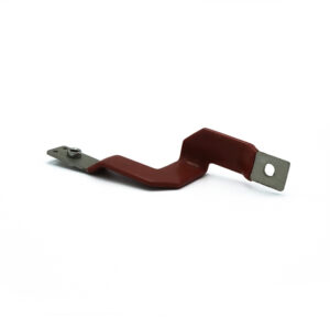
Core Technology & Functionality
Engineered for PCB-mounted hybrid sockets, this 0.5mm stainless steel housing overcomes industry-critical forming challenges:
Ultra-Narrow 90° Bending: Achieves bends narrower than material thickness via multi-stage forming with pre-score lines and pressure ribs at every station to eliminate deformation.
Burr-Free Trimming: Proprietary upward waste-cutting + pneumatic ejection ensures ±0.05mm dimensional accuracy and smooth edges.
Tear-Form Pin Contacts: Tungsten steel punch inserts replace conventional R-angles to enable seamless bend marks and EMI-shielded pin alignment.
Primary Function:
Provides electromagnetic shielding and mechanical stability for high-density PCB connectors in compact electronics.
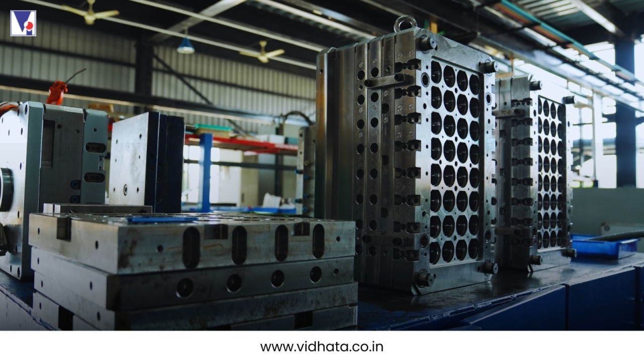
Products details
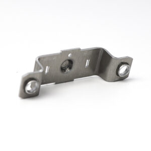
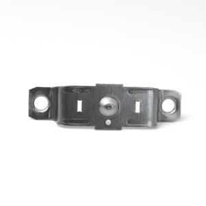
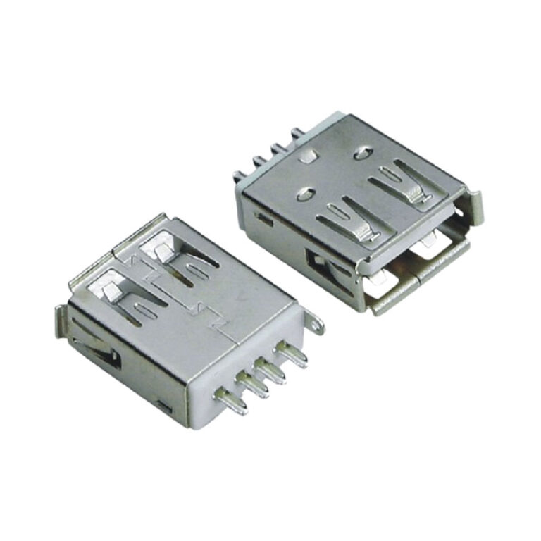
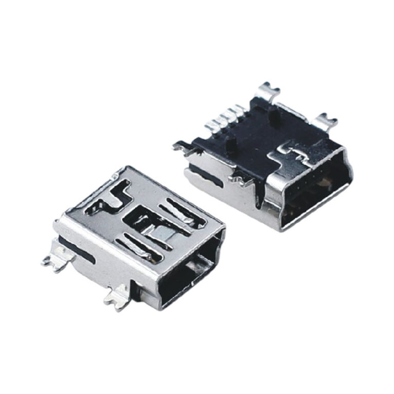
SMT Socket Housing with Precision Metal Bending
This advanced SMT socket housing uses 0.5mm stainless steel formed with ultra-tight 90° bends—achieved through multi-stage tooling and pre-score lines. Our design eliminates deformation and distortion, enabling housing widths narrower than material thickness—a known industry challenge.
Key to this breakthrough is the integration of pressure ribs at each station, maintaining bend accuracy even at micron levels. This level of precision metal bending ensures mechanical fitment and electromagnetic performance for space-constrained PCBs.
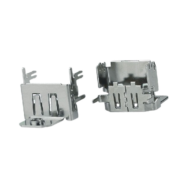
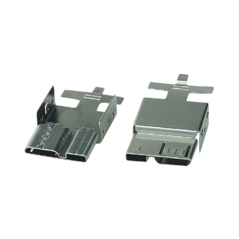
Zero-Burr PCB Shielding with Tear-Free Edges
To achieve zero-burr PCB shielding, we apply a proprietary upward shearing and pneumatic ejection technique. The result: ±0.05mm dimensional tolerance and scratch-free edges (Ra ≤ 0.4μm). Our tear-form punch structure removes the need for R-angle clearances, preventing EMI leakage at pin contacts and preserving circuit integrity.
This smooth, burr-free finish is critical for connectors in 5G RF modules, GPU sockets, and SSD shields, where debris or misalignment could compromise data flow or mechanical retention.
Applications Across 5G, IoT, and Medical Devices
Our SMT socket housing is the ideal choice for:
-
5G/6G infrastructure: base station RF module shielding, high-frequency sockets
-
Industrial IoT boards: edge computing device interfaces, real-time sensor housings
-
Consumer electronics: high-speed GPU connectors, SSD PCB covers
-
Medical devices: ultra-compact wearable and diagnostic PCBs
With electromagnetic shielding, mechanical retention, and ultra-fine pin-spacing accuracy (±0.03mm), the part supports high-speed data, RF stability, and mechanical reliability.
Fully Automated Production with Rapid Customization
Our in-line optical inspection guarantees 100% pin alignment. Combined with robotic ejection and press-control systems, we ensure consistency across high-volume orders.
We offer:
-
Custom pin pitches and cutout geometry
-
7-day prototype turnaround
-
Tungsten punch inserts for sharp, tear-free edge formation
This is precision metal bending brought into scalable, automated manufacturing.
Applications
5G/6G Infrastructure: Base station RF module housings, antenna array sockets.
Industrial IoT: Sensor control boards, edge computing device interfaces.
Consumer Electronics: SSD connectors, GPU socket shields in laptops/consoles.
Medical Devices: Miniaturized monitoring equipment PCBs.
5 Reasons to Choose Us
Bending Revolution:
Solved “width < thickness” bending paradox via pressure-rib reinforced multi-step forming.
Zero-Contact Trimming:
Air-blown waste removal prevents surface scratches (Ra ≤ 0.4μm).
Full Automation:
In-line vision inspection guarantees 100% pin-spacing accuracy (tolerance: ±0.03mm).
Rapid Customization:
7-day prototype turnaround for custom pin configurations.
Explore advanced PCB shielding and connector design guidelines from IPC International